|
Dualbeam
FIB system
- integrates both the ion beam and
electron beam into one system
Electron
column is used to image the sample. The ion beam can be used to raster
over the surface similar to electron beam in a scanning electron
microscope (SEM). The focused ions will mill away the sample through
atomic collision process.
An important capability derived from the FIB system’s milling capacity,
is the creation of thin lamella for TEM. As the position of the ion
beam can be controlled precisely, the lamella can be located at
specific position that is of interest to the user. More ever, the
milling is an atomic collision process. The lamella preparation
procedure is therefore material independent.
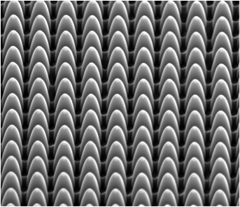
Another capability is the formation of nanostructures for nanodevices.
Besides the milling capabilities, by adding a gas delivery system, it
can convert the ion beam system into a deposition system.
Process control and failure analysis capabilities offered by FIB
provide the fastest possible route-cause data to solve site specific
failure modes.
|